Energy-Resolving Time-of-Flight Mass Spectrometry for Bulk Plasma Analysis
Watzek et al.
JASMS
DOI: 10.1021/jasms.4c00140
This recent publication in collaboration with Swiss Federal Laboratories for Materials Science and Technology (EMPA) and the Berner Fachhochschule (BFH) showcases our newly designed Semicon Process Solution energy-resolving time-of-flight mass spectrometer (TOFMS).
The field of materials science, particularly thin film deposition processes, has significantly advanced beyond simply controlling chemical composition to managing the deposition environment. The influence of process parameters on deposited film properties is well documented, with studies highlighting the role of energetic species in phenomena like ion bombardment-induced stress in AlN films and the formation of sp3 bonds in diamond-like carbon films during magnetron sputtering.
Understanding the energies of ionic species is crucial for linking microstructural and crystallographic changes in thin films under various deposition conditions, such as comparing direct current magnetron sputtering (DCMS) with high power impulse magnetron sputtering (HiPIMS), the effect of substrate bias, and different plasma source combinations. These conditions impact not only single layers but also the interfaces in multilayer structures, necessitating a comprehensive understanding of deposition conditions for precise material and device manufacturing.
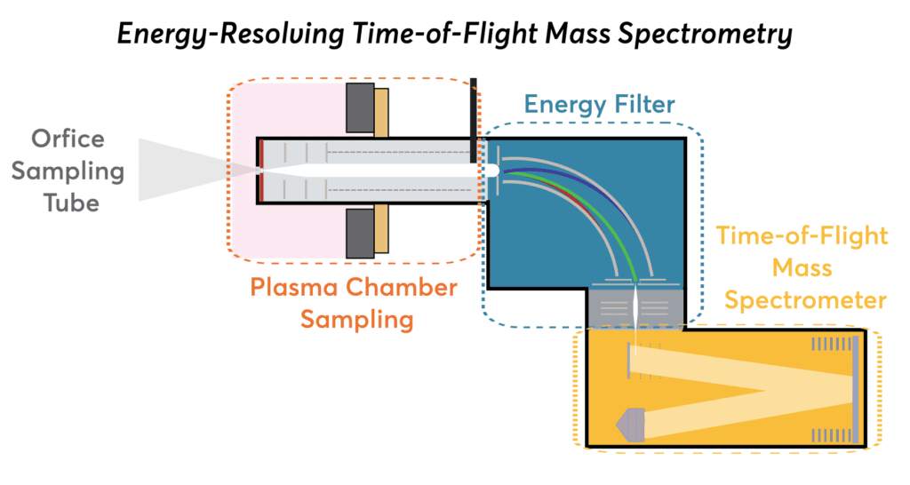
This work introduces an energy-resolved TOFMS system combined with an electrostatic energy analyzer (ESA) to identify plasma ion species and their energy-to-charge (E/Q) ratios. ESAs use electric fields to bend and focus ion beams, with cylindrical deflector plate analyzers focusing in one direction and additional electrodes enabling dual-direction focusing for a narrow E/Q ratio band. This enhances quantitative and high-resolution mass spectrometry. The new TOFMS system, designed for in situ characterization of various deposition environments, is validated through comparison with other plasma analytical devices like Langmuir probes and retarding field energy analyzers. The system’s design and operation are detailed, demonstrating its capabilities for advanced thin-film deposition analysis.
This study further highlights the versatility and capabilities of our Semicon Process Solutions for process monitoring and control. This newly developed instrument provides a versatile tool for analyzing complex plasma processes with multiple energetic and chemical species, making it especially useful in thin film deposition processes and technology. While primarily applied in physical vapor deposition (PVD) and magnetron sputtering, this instrument is also beneficial for plasma enhanced chemical vapor deposition (PECVD) and atomic layer deposition (PE-ALD). Additionally, it can be used in propulsion thrusters to determine the energy distribution of ions in propulsion plumes. It provides superior mass-to-charge (m/Q) and energy-to-charge (E/Q) resolution compared to traditional QMS systems, facilitating the monitoring of plasma processes and the identification of process instabilities.
