Nanostructure and Optical Property Tailoring of Zinc Tin Nitride Thin Films through Phenomenological Decoupling: A Pathway to Enhanced Control
Hain et al.
ACS Appl. Nano Mater
DOI: 10.1021/acsanm.3c06178
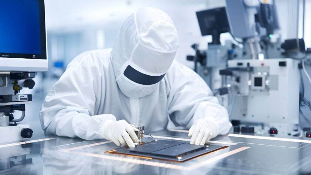
This recent publication in collaboration with the Swiss Federal Laboratories for Materials Science and Technology (EMPA), the Swiss Federal Institute of Technology in Lausanne (EPFL) and the Berner Fachhochschule (BFH) showcases our newly designed Semicon Process Solution energy-resolving time-of-flight mass spectrometer (TOFMS), used in conjunction with other in-situ diagnostic techniques to monitor changes during thin film sputtering processes.
Advancing thin film fabrication processes is crucial for tailoring the chemical composition, structure, and properties of materials to meet specific application requirements, such as in photovoltaics and passive radiative cooling. Key developments like high-power impulse magnetron sputtering (HiPIMS) and electron cyclotron resonance (ECR) microwave (MW) sources facilitate phenomenological decoupling, allowing the separation of effects such as heat from plasma density. This study examines the feasibility of combining ECR MW plasma with HiPIMS for co-sputtering zinc tin nitride (ZTN) thin films, a semiconductor with promising optoelectronic properties. The goal is to investigate how variations in the deposition environment—such as plasma potential, ion energy, and plasma chemistry—affect the nanostructure and optical properties of ZTN films, building on previous research into temperature-sensitive materials.
To this end, our newly developed energy-resolving TOFMS system was employed to analyze plasma chemistry and ion energy distribution. It provides mass spectra up to 500 Th with varying resolving powers (500 for low m/Q and 1000 for heavier ions) and measures ion energy-to-charge (E/Q) values using an electrostatic energy analyzer. Ions were sampled through a 20 μm orifice and transferred to the mass spectrometer under low pressure conditions.
Zinc tin nitride (ZTN) films were successfully deposited using MAR-HiPIMS with varying plasma power and substrate bias. The process consistently produced stoichiometric ZTN films, with enhanced control over film texture due to the microwave plasma’s role in forming ionic nitrides and narrowing ion energy ranges. Despite optical anisotropy, the films’ properties were comparable overall due to minor lattice changes. MAR-HiPIMS shows promise for precise film tailoring, with potential benefits for optics and photovoltaic applications.
This study highlights the versatility and capabilities of our Semicon Process Solutions for process monitoring and control of thin film sputtering processes. Our newly developed instrument provides a versatile tool for analyzing complex plasma processes in real-time, offering new insights into deposition processes with multiple energetic and chemical species.
