Ben Bensaoula
TOFWERK Switzerland
Introduction
Atomic layer deposition (ALD) is rapidly becoming a standard technique for a wide range of thin film materials and is an essential tool in the semiconductor sector. ALD relies on self-limiting surface reactions of two gaseous reactants in sequential mode to obtain sub-nanometer control of the thickness and conformity of a thin film, even on substrates with complex 3D geometries. The physicochemical properties of the deposited films depend mainly on surface decomposition reactions and growth mechanisms. Therefore, it is important to fully characterize and understand these processes and utilize metrology tools that shorten the process optimization cycle and provide real-time monitoring and control in a production environment.
Semicon Process Solutions for ALD
This application note presents the integration of a TOFWERK Semicon Process Solution in an atomic layer deposition system (SC-1, from Swiss Cluster AG, Thun, Switzerland) for real-time monitoring of thin film fabrication processes. The Semicon Process Analyzer simultaneously detects all ionized molecules with isotopic resolution, greater than 105 dynamic range, and mass spectral acquisition rates up to 1 kHz. Because the chemical data acquisition is conducted in-situ, the results of applied deposition parameters can be monitored instantly, allowing for immediate modifications of the process experimental conditions like temperature and pulsing/purging times. In addition, any process excursion from optimal conditions or equipment malfunction is also detected. This in-situ acquisition with the Semicon Process Analyzer is a great advantage over post-mortem (ex-situ) chemical and structural characterization methods, which are characterized with significant delays.
Experimental Set Up
The ALD process was performed using a novel compact cluster system, SC-1, which combines ALD and PVD. This study used only the ALD module of the SC-1. The substrate temperature was set to 120 °C. Trimethylaluminium, Al(CH3)3 (TMA, 98 % purity, from Strem) and DI H2O were used. These two gas precursors are commonly used for depositing Al2O3, a model ALD system. The chemistry of this process has been broadly analyzed in numerous studies and served for the evaluation of results presented in this work. Both precursors were delivered at room temperature to the deposition chamber and 99.9995% purity argon (from Air Liquide) was used as the purging gas.
The experiments consisted of 20 ALD cycles. Each cycle included a 50 ms pulse of TMA and a 30 ms pulse of H2O without Ar carrier gas, aiming that only the gases of interest are introduced to the chamber. Between the gas precursor pulses, a 50 sccm argon gas purge over 30 s was provided.
Results
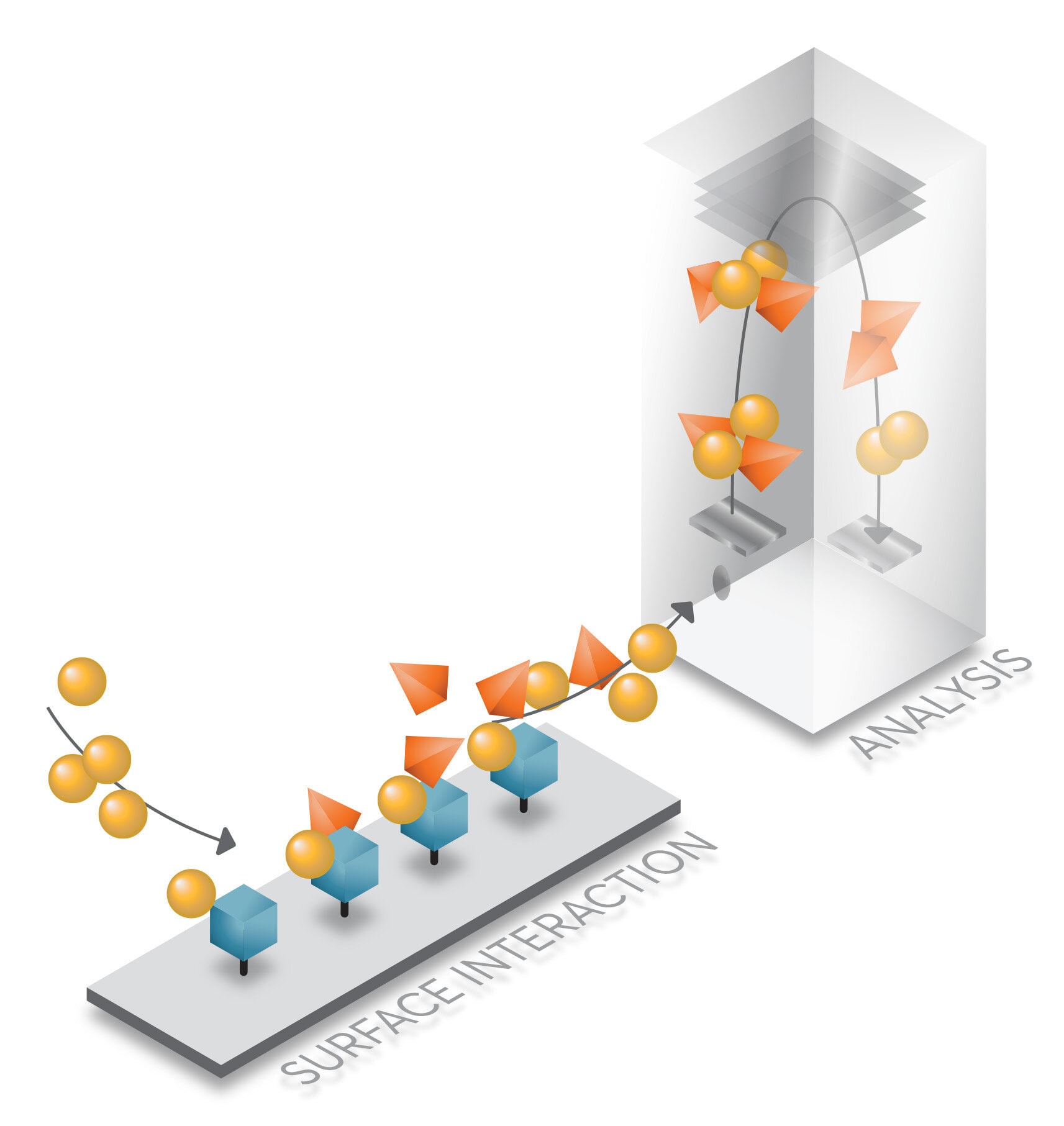
In ALD, the reactions between the sequentially introduced gas precursors and the surface led to the release of by-products as described in Figure 1. The chemistry and amount of these by-products provide important information on the fundamental reaction mechanisms and give isight for the development of monitoring protocols for reliable and reproducible processes at an industrial scale.

We show that the Al2O3 deposition using TMA and H2O can be characterized based on the signal distributions measured mainly at m/Q = 16 Th, 18 Th, 27 Th, and 40 Th, corresponding to the TMA Al (27 Th), H2O (18 Th), the by-product CH4 (16 Th) and the Ar carrier gas (40 Th). However, the ability to detect all masses simultaneously, as shown in Figure 2, allowed us to observe additional by-products that were not previously detected and, without the high mass resolution and accuracy of the Semicon Process Analyzer, would have been difficult to identify otherwise.

Another important feature afforded by Semicon Process Solutions is the ability to monitor the time variation of all species present in the reactor, as demonstrated in Figure 3. Figure 4 shows the measured characteristic values of the 27Al signal distribution, i.e., the 27Al signal peak amplitudes when the TMA valve was open, and their full widths at half maximum (FWHM). The variations of these two values indicate that the amount of delivered TMA varied between cycles. Although the ALD process is self-limiting and the excess of the TMA precursor does not induce an increase in the layer thickness, precursor consumption can be optimized. By contrast, a lower precursor amount will yield partial monolayer deposition and result in a rough surface morphology and less than ideal interfaces when deposition of a heterostructure is the goal. As such the real-time quantification of cycle-to-cycle ALD process reproducibility, made possible with Semicon Process Analyzers, is important in both process optimization (R&D) and production.


Conclusion
As presented in this application note, incorporating a Semicon Process Analyzer within an ALD system allows for simultaneous, real-time detection of all ionized molecules and fragments. Therefore, any process deviation from optimal or malfunction can be detected at an early stage, and consequently the deposition parameters, such as precursor temperature, pulse duration and pressure can be corrected immediately to ensure deposition of the intended thin film chemical structure.
The advantages of in situ Semicon Process Solutions for ALD processes will extend to other deposition techniques, such as chemical vapor deposition and to etch applications for process optimization, monitoring and control. End-point detection could be implemented for complex interfaces such as transitions involving binary, ternary and quaternary alloys. Furthermore, the high acquisition speed is critical for sources operating in pulsed modes and processes involving deposition and etch of nanolayered stacks. Semicon Process Solutions can be broadly applied as a monitoring tool in other semiconductor processes, where chemical species in complex gaseous environments need to be accurately assigned and their time variation measured.
Acknowledgment
We would like to thank EMPA Eidg (Thun) and Swiss Cluster (Thun) for their data collection and analysis contributions to this application note.

